Photodiode and circuit design
Design of the photodiode and its readout circuit, both simulated with your device model to verify they meet the spec.
Optical and circuit design, EUV and DUV thin-film optics, and the datasheets, application notes, 3D models and drawings that support photonics components.
λ 13.5 nm
Extreme ultraviolet
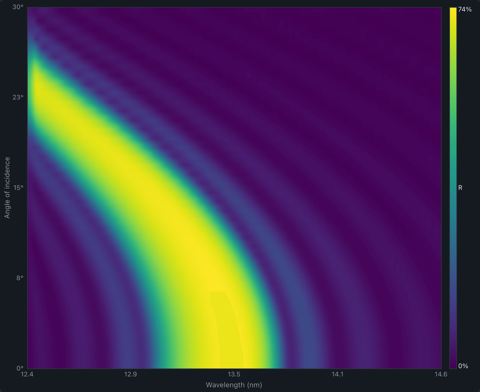
Mo/Si multilayer mirrors and free-standing filters, modeled with CXRO data
EUV and DUV opticsDesign of the photodiode and its readout circuit, both simulated with your device model to verify they meet the spec.
Multilayer mirrors and thin-film filters for 13.5 nm, 193 nm and 248 nm, modeled in the EUV Insight browser app.
Datasheets, application notes and test reports that give engineers the conditions and worked examples they need.
Browser calculators, 3D models and drawings, sales material and trade show booths, plus market and competitor research.
Design and modeling of thin films for 13.5 nm transmission and reflection: free-standing filters on their support mesh, and Mo/Si multilayer mirrors with the period and capping layer set for the required angle and bandwidth. Spectral purity modeling covers how much of the source’s deep-UV and infrared light passes the filters to the mask and wafer.
EUV Insight, a browser app for EUV thin films and multilayers built by Jezdan Gomez, is used to compare materials and thicknesses, run thickness tolerances and export spectra for reports and datasheets. DUV coatings and filters for 193 nm and 248 nm are also covered.
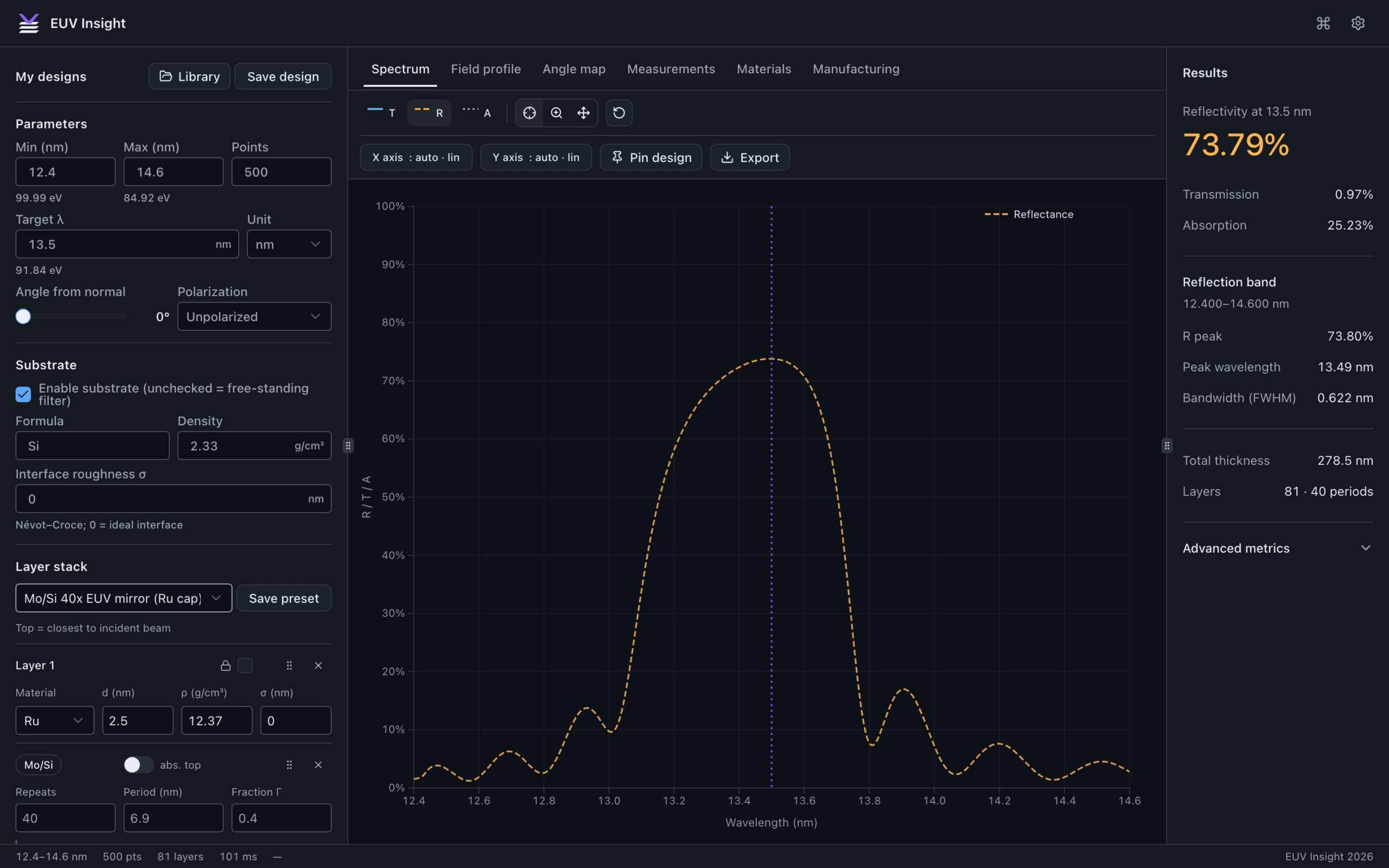
Values from the results panel in the screenshot, for a Ru cap on 40 Mo/Si bilayers with a 6.9 nm period on a Si substrate.
Photodiode front-end design from the device model to the finished board: TIA configuration, bias and filtering, noise and bandwidth, and SPICE and MATLAB simulation with your photodiode as a device model to verify the circuit meets the requirements.
Deliverables continue through the KiCad schematic and PCB layout, the 3D model and a datasheet written from the same model and test data. Available as individual steps or as the complete chain.
Application notes, selection guides and datasheets, plus CAD and circuit design, for parts that work anywhere in this range.
For makers of multilayer mirrors, excimer optics and lithography subsystems: application notes on reflectance and layer tolerances, and datasheets for DUV coatings and CaF₂ optics. EUV Insight is the thin-film design tool for this band.
For laser, filter and microscope optics makers: selection guides that match filter sets to laser lines, datasheets that state their test conditions, and an AOI shift calculator for your filters.
For diode laser, fiber and LiDAR optics makers: application notes on TEC control and wavelength drift, such as the TEC heat-load sample, product pages for telecom and LiDAR filters, and photodiode front-end circuit design.
For IR material, lens and QCL makers: transmission and coating datasheets, and lens selection guides for germanium and chalcogenide glass.
Each sample cites its public references, and every figure and table in it is computed from code.
Application note, 8 pages, with a TEC heat load calculator.
Open the PDF (opens in a new tab)Selection guide and white-paper example, 10 pages, with optical density and angle shift calculators.
Open the PDF (opens in a new tab)A thin datasheet for a filter family, rewritten with its test conditions, typical values kept apart from limits, and curves drawn from code.
Open the PDF (opens in a new tab)EUV Insight is a browser app for optics engineers designing EUV thin films and multilayer optics.

Technical documents, browser calculators and circuit design, plus CAD files prepared from your released drawings.
Photonics and optics component makers, typically 20 to 400 people, that need application notes, product documentation or tools for selecting parts.
The same work suits makers of precision components in test and measurement, scientific instruments, motion and industrial automation.
Start with one small project or a full kit. Every price is agreed before work starts.
A capability card, a datasheet refresh, a technical article or a product-page rewrite.
One application note with a worked example and supporting calculations.
Datasheet refresh, product page, technical article, three posts and the launch email, timed to your launch.
Application note, selection guide, a design calculator, a sales one-pager and a technical FAQ.
Monthly retainers are available for ongoing documentation and calculator work.
Technical content written and checked for booths, banners, brochures, catalogs and booklets, with design by Pento Agency (opens in a new tab), who designed and built this site. One point of contact from the brief to the print-ready files.
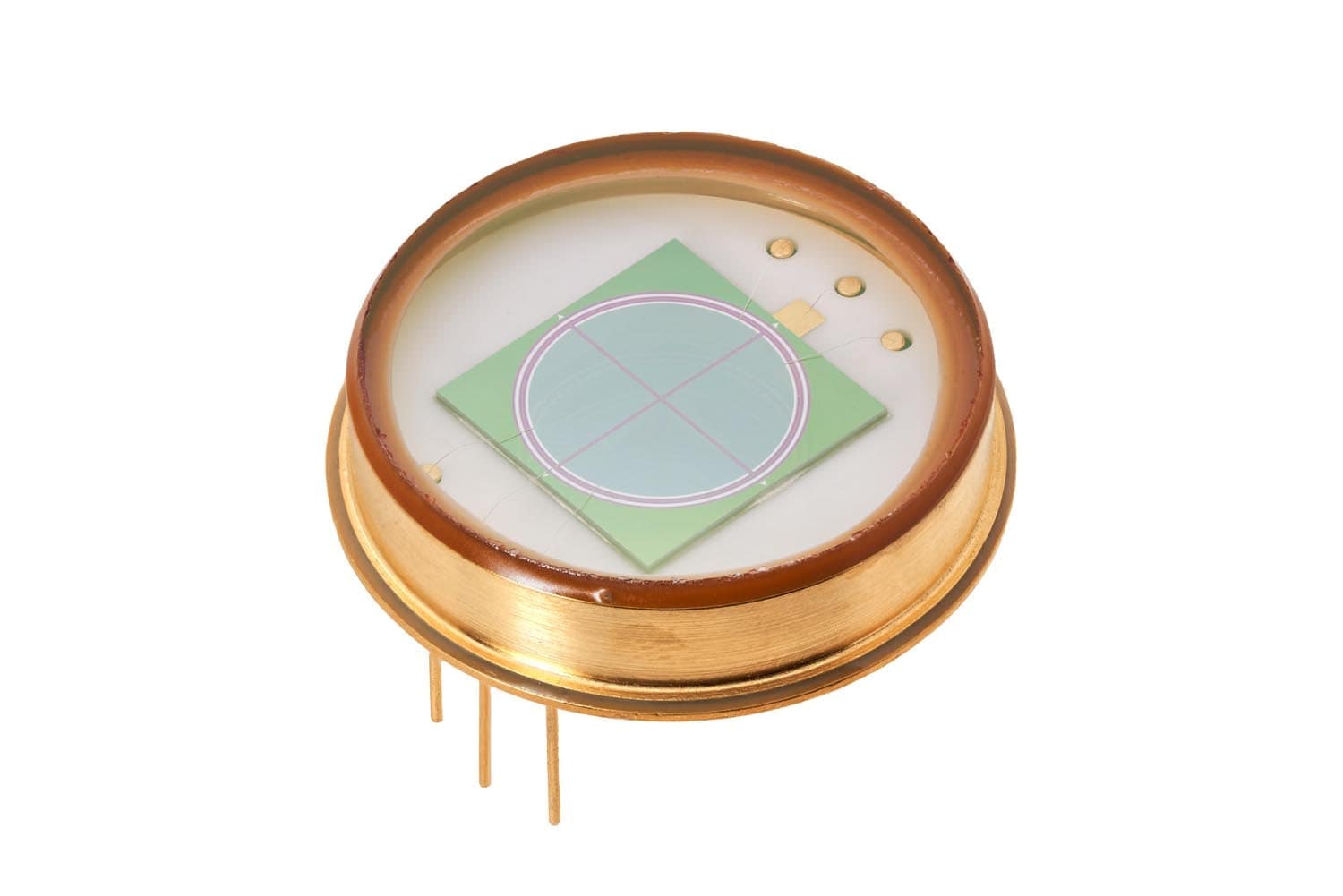
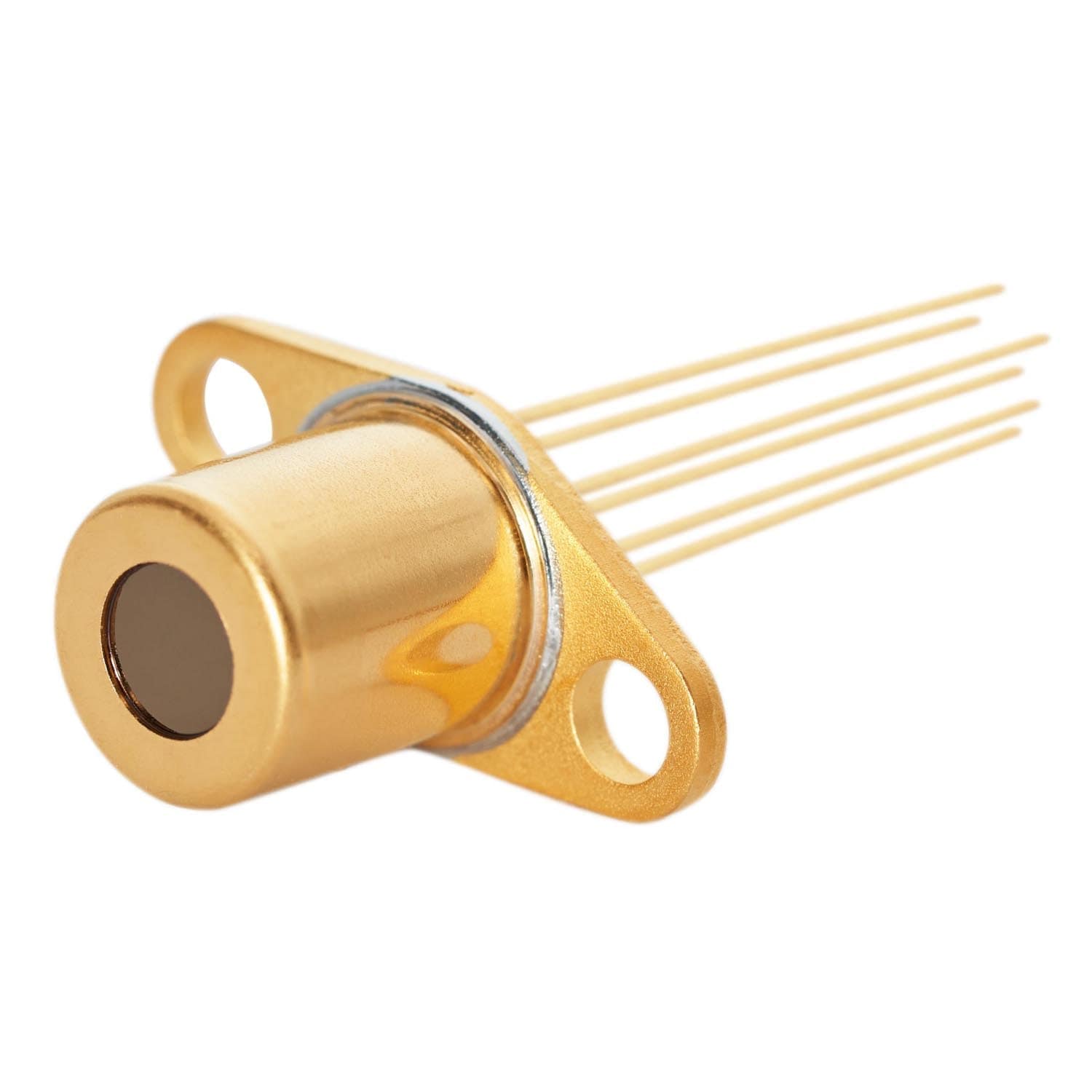
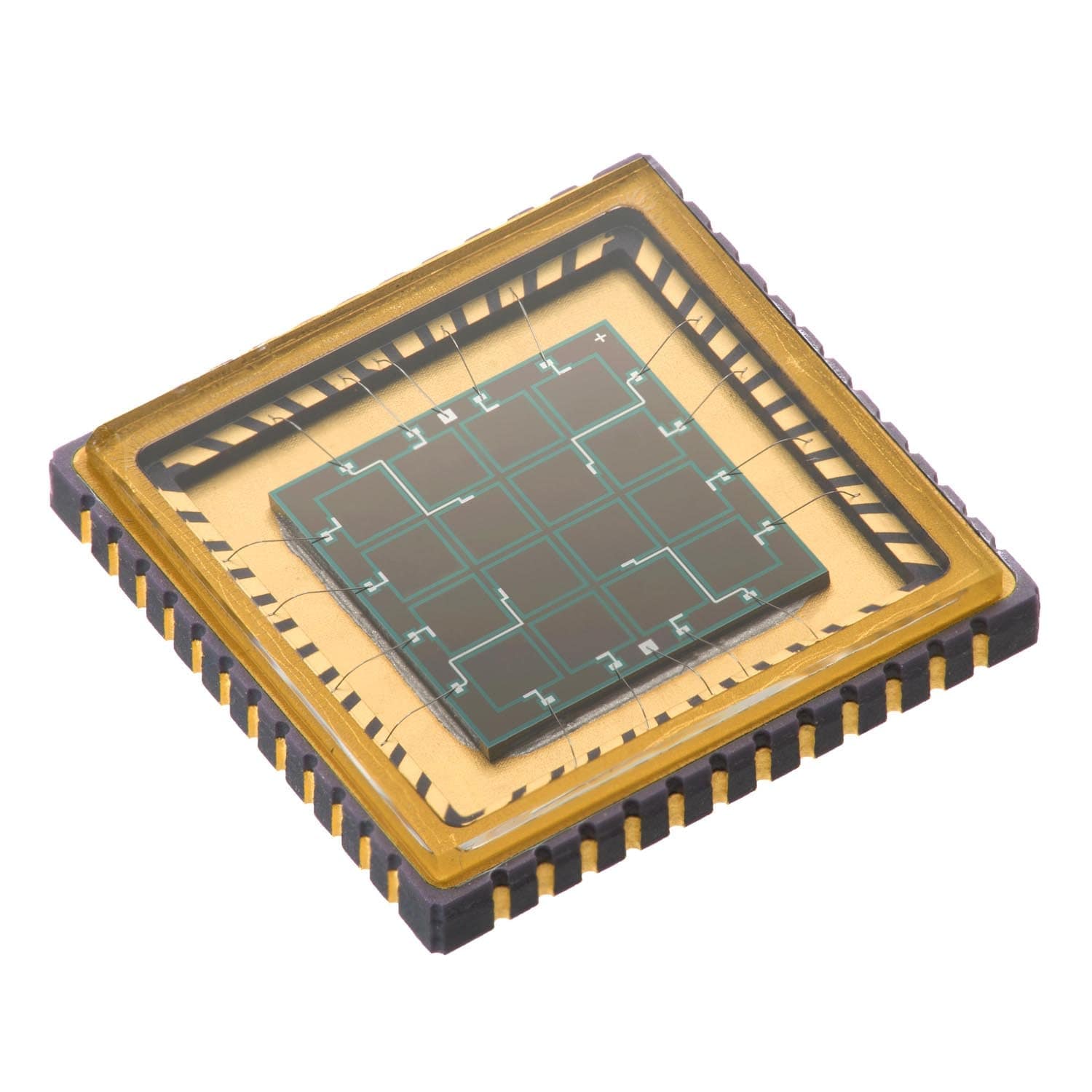
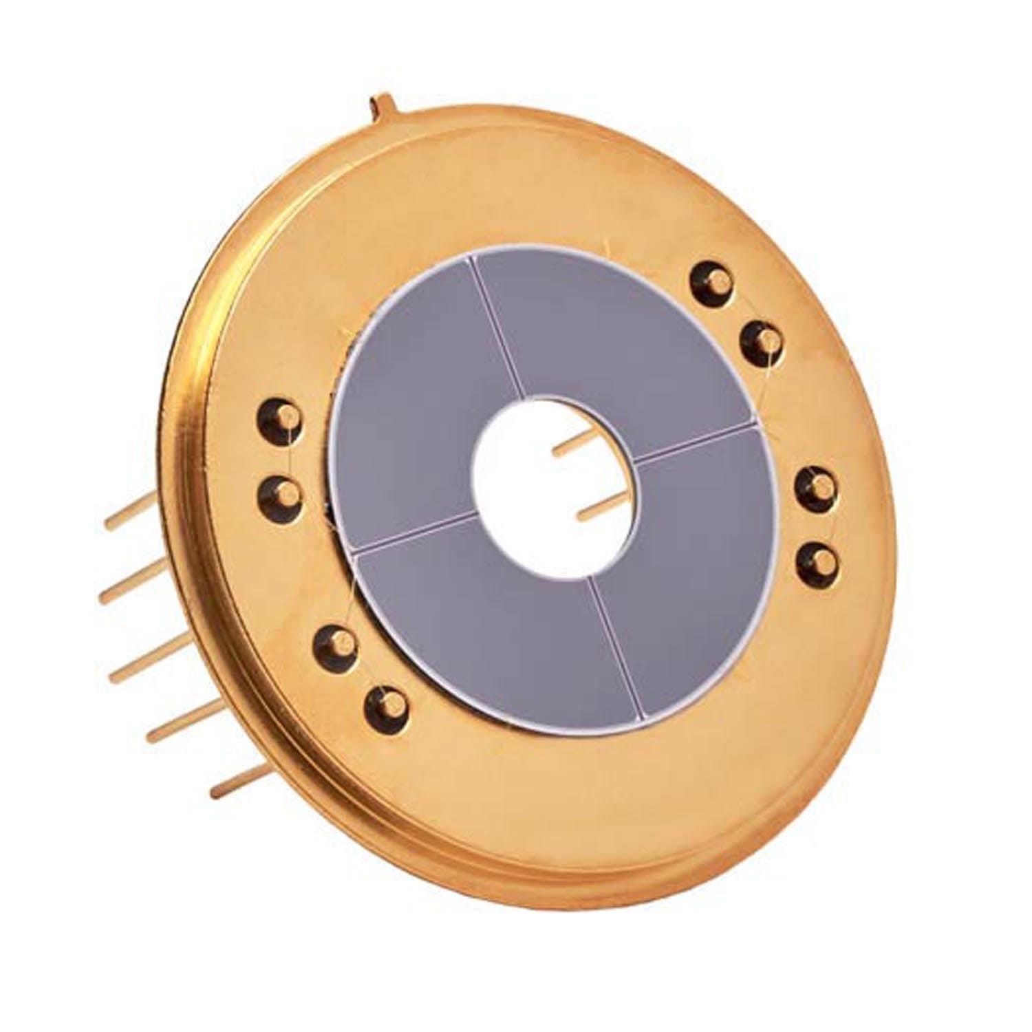
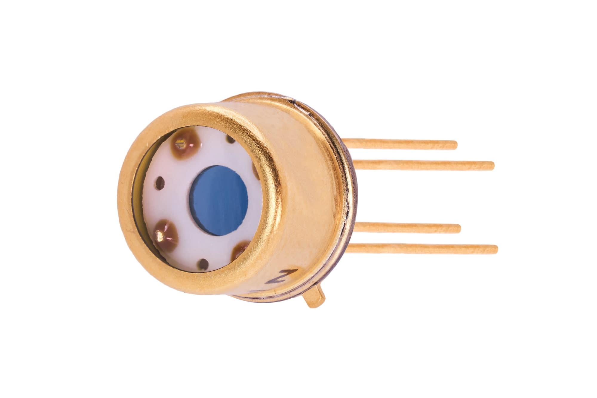
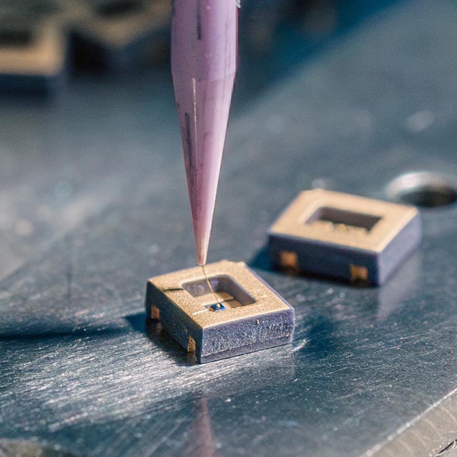
Macro photographs of optical and electronic parts on white, for datasheets, product pages, catalogs and trade-show graphics.
Get a one-page comparison of your technical content with two competitors, three recommended documents or tools, and a price for the first project.